Wave Photonics has raised £4.5m in a finance round led by the UK Innovation & Science Seed Fund and Cambridge Enterprise Ventures, with participation from the Redstone and QAI Ventures’ Quantum Fund, Kyra Ventures, and Deep Tech Labs.
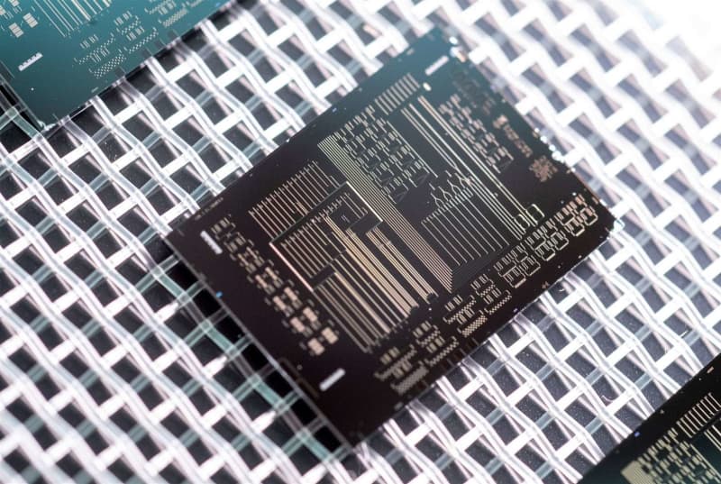
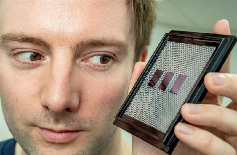
The Cambridge-based deep tech start-up develops chip photonics designs for quantum technologies, sensors, and datacentre applications. The circuits are driven by integrated photonics using light – and uses the same scalable process used to make semiconductor electronics chips.
“A conventional semiconductor foundry can make integrated photonic chips with their existing equipment, although they do have to develop/change the process from the electronics one,” says James Lee, the CEO who co-founded Wave Photonics. “It’s one of the reasons that the field is exciting – it’s possible to leverage the scale and R&D that’s gone into the semiconductor industry to make chips that use light instead.”
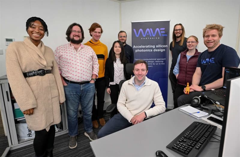
The sensational development has been curated by James with fellow Cambridge Quantum Photonics PhD Matthew Anderson, plus Mateusz Kubica, CTO, a former quantitative finance VP with 10 years experience in mathematical and computational modeling.
The new investment will enable the company to take its technology from a research manufacturing line to a commercial foundry, with a particular focus on solutions for frontier applications such as quantum technologies and biosensing.
“The team has spent the past few years building and experimentally validating our design technology,” says James. “It’s exciting to have the resources to begin deploying it to solve real industry problems.”
Already, some photonics processes are available from large electronics foundries such as New York-based GlobalFoundries, but there are also dedicated photonics fabs like AMF in Singapore or Ligentec in Switzerland.
“Overall, what this round really marks is a change in focus,” adds James. “So far, it’s been a 90 per cent-plus focus on R&D and proving that the technology we’re building does what we wanted it to – we’ve been working with a research foundry in Southampton to do all of the testing on this. For this next stage, we’ll be working with a larger commercial foundry in either the US or Asia – we’re still in discussions to determine which one.
“We won’t be an OEM, more of a design/IP company – it’s not a 100 per perfect analogy, but the best one is a bit like an Arm for photonics. In the same way processor designs from Arm make it possible for many more chips to be built, from Apple chips to chips that control washing machines, we want to make the full space of possibilities for integrated photonics more accessible.”
Dr Christine Martin, head of ventures at Cambridge Enterprise, said: “Integrated photonics is poised to disrupt high-value industries ranging from quantum computing to bio-sensing, and Wave Photonics’ team and technologies are in a great position to enable and accelerate the adoption of next-generation integrated photonics products.”